|
Tokyo, July 9, 2001 -- Hitachi, Ltd. (TSE: 6501) today announced two
AND-type flash memories employing a small CSP package, the 128-Mbit
HN29W12811BP-60 and 256-Mbit HN29V25611ABP-50, for embedding in portable
products such as third-generation(3G) mobile phones, PDAs, and digital
cameras. Sample shipments will begin in July 2001 for the 128-Mbit
model and in August 2001 for the 256-Mbit model in Japan.
These two new products feature a mounting area approximately 43% that
of Hitachi TSOP products, and are provided with a development reference
kit to simplify embedded system design. These features will make it
possible to reduce the size of systems incorporating large-capacity
flash memory, and also achieve shorter development times.
[Background]
With the increasing functionality of mobile phones and the growing
volumes of information they are required to handle, including e-mail
and WWW contents, the capacity of their built-in memory also continues
to expand. 3G mobile phones using W-CDMA, cdma2000, or a similar system,
in particular, can be expected to require at least 128-Mbit flash
memory capacity for data storage.
Following on from Hitachi's currently available 128-Mbit and 256-Mbit
AND-type flash memories in TSOP packages, the company has now developed
the industry's smallest 128-Mbit and 256-Mbit flash memories employing
a CSP package for embedded systems such as mobile phones, PDAs, and
digital cameras that require a compact, lightweight design.
[About these Products]
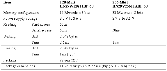
The 256-Mbit HN29V25611ABP-50 AND-type flash memory achieves a small
chip size through the use of a 0.18 µm process, and is housed
in an 11.26 mm × 9.22 mm, 72-pin CSP that requires only approximately
43% of the mounting area of Hitachi's flash memory TSOP packages.
In addition, the power supply voltage of 2.7 V to 3.6 V offers low
system power consumption.
The 128-Mbit HN29W12811BP-60 AND-type flash memory employs a 0.25
µm process, operates on a power supply voltage of 3.0 V to 3.6
V, and uses the same 72-pin CSP package as the 256-Mbit product.
[About the Development Environment]
“An AND flash memory development reference kit” is available
to simplify the development of systems incorporating these two flash
memories. Since simulation can be carried out on a PC, the system
performance can be evaluated during the design stage.
In addition, functions such as AND-type flash memory operation management,
previously performed by hardware by connecting a dedicated controller,
are now managed by software for purposes of embedding in a small end-product.
The software is provided as C-language source code with a wide range of
microcomputers.
< Typical Applications >

< Prices in Japan > (For Reference)

< Specifications >

|