 |
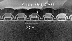
| AG-AND Flash Memory Cell |
Tokyo, December 4, 2001 — Hitachi, Ltd. (TSE: 6501) today announced
the development, in collaboration with its Central Research Laboratory
and its Device Development Center, of an AG-AND (Assist Gate-AND)
type flash memory cell as high speed next generation AND-type flash
memory for gigabyte-generation.
Through the use of Hitachi's originally developed field isolation
method employing an assist gate for preventing inter-cell interference,
this cell enables high-speed writing even with a Multi Level Cell
configuration, and 10-Mbyte/second writing is possible with a 0.13
µm process.
In addition, the chip size can be further reduced, and large-volume
data can be recorded at high speed in a small flash memory or flash
card. This will help reduce downloading time when large-volume digital
content such as movie content is distributed in the future using broadband
transmission.
[Background]
Flash memory for date file storage such as AND-type flash memory is
already widely used as large-volume storage ROM/cards not only in
digital still cameras and portable music players, but also digital
video cameras, mobile phones, PDAs, and similar portable products
and information devices of various kinds. In addition, demand for
such memory is growing in industrial and communication fields as a
replacement for small-capacity HDDs. Against this backdrop, the most
important key points in flash memory development are reduction in
chip size through Multi Level Cell technologies as well as continuing
progress in implementing finer processes in order to achieve greater
capacity, smaller size, and lower cost.
Meanwhile, there has been the problem of the programming time of a
Multi Level memory cell being longer than for a conventional binary
cell. In a digital camera with around two to three million pixels,
the current programming time of around 1 Mbyte/second is sufficient,
but the use of higher pixel counts in digital cameras and future distribution
of various kinds of digital content using broadband transmission will
require high-speed writing on the order of 10 Mbytes/second. To meet
these demands for small size and high speed, Hitachi has developed
a new AG-AND memory cell for implementing flash memory that makes
possible high-speed writing in a Multi Level mode.
[Details of Technologies]
| (1) |
Smaller cell size
In order to achieve not only a finer process but also a smaller
cell size, the cell structure has been changed from the conventional
SGI (shallow groove isolation) type to Hitachi's original field
isolation type. The use of an AG-AND type cell structure in which
assist gates for preventing inter-cell interference and floating
gates are combined alternately has made it possible to achieve
a cell area of 0.052µm2 (on a bit basis) with a 0.13 µm
process, representing a size reduction of more than 50% compared
with a conventional SGI type 0.18 µm process product. |
| (2) |
High-speed writing
In order to achieve fast Multi Level Cell flash memory, in an
AG-AND type cell the programming method has been changed from
conventional F-N tunneling to hot electron injection. Injecting
hot electrons from the source side improves the floating gate
injection efficiency, making possible high-speed parallel writing.
In the commercial development of 0.13 µm process products,
using a 4-bank configuration within the chip enables a high speed
of 10 Mbytes/second to be achieved. A single standard music CD
(around 64 Mbytes by using compression technology ) can be downloaded
to a flash card in approximately 6 seconds, and it is possible
to offer the market a small card containing one or two chips capable
of 10 Mbyte/second writing, the current target for small flash
cards such as MultiMediaCardTM* products. |
Future plans include the commercial development of gigabit-class
flash memory using the present technologies and various kinds of flash
cards and systems using such memory.
The above achievements will be announced at the 2001 International
Electron Devices Meeting to be held in Washington D.C., U.S.A., starting
December 3rd.
Notes:
* MultiMediaCardTM is a trademark of Infineon
Technologies AG of Germany, and is licensed to the MMCA (MultiMediaCard
Association). Hitachi is an MMCA board member.
http://www.mmca.org/
|