|
||
| Dual-Power-Supply Circuit Technique Achieving both High-Speed Performance and Low Power Dissipation of Large-Scale Integrated Circuits |
| — Implemented by means of well sharing and domino type level conversion circuit techniques — | ||||||||
Tokyo, February 10, 2003— Hitachi, Ltd. (TSE: 6501) today announced the development of a circuit technique that is effective in achieving both high-speed performance and low power dissipation in large-scale integrated circuits (LSIs) such as system-on-a-chip (SoC). With a test chip of Arithmetic Logic Unit (ALU)--a main circuit of a microprocessor--using this technique showed the saving in power dissipation of approximately 25% compared with single-power-supply circuitry, while the decrease in operating frequency was kept to a mere 2.8%. This technique has been jointly developed by Hitachi, Ltd. and the University of California, Berkeley (UC Berkeley). The results achieved will be announced jointly at the International Solid-State Circuits Conference (ISSCC) to be held from February 9 in San Francisco, U.S.A. The power dissipation of LSIs, the mainstay of IT devices, continues to increase in line with the trends of higher performance and functionality, and technologies for reducing power dissipation are very important issue in the future development of increasingly larger-scale integration. An effective method of achieving lower power dissipation is to use the lower supply voltage of LSIs, but simply using a lower voltage also causes a drop in the operating frequency. One technique that has been proposed to solve this problem is the use of dual-power-supply circuitry, in which a comparatively high voltage is used for circuits requiring high speed, while a lower voltage is used for other circuits. However, with conventional dual-power-supply circuit techniques, the layout and wiring of the nominal-voltage circuits and low-voltage circuits is complex, and there is a further problem of increased signal delay times due to the voltage level conversion circuitry for converting the lower voltage to the higher voltage. Against this background, Hitachi and UC Berkeley, conducted joint research into a circuit technology capable of both increasing the operating speed and decreasing the power dissipation of an LSI. The two developed a basic technique for implementing a dual-power-supply system, and confirmed its effectiveness. Features of this jointly developed technique are as follows.
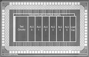
A test chip of 64-bit ALU has been constructed, using a 0.18-micron CMOS process, to verify the effectiveness of the above-described technique. Tests confirmed that, in dual-power-supply operation, power dissipation fell by approximately 25% with a decrease in operating frequency of only 2.8%, and by approximately 33% with a decrease in operating frequency of 8.3%, compared with the power dissipation at the maximum operating frequency of 1.16 GHz when the dual power supplies were made equivalent to a single power supply, using the same voltage. Moreover, leakage current in the standby state was confirmed as falling by approximately 42% compared with a single-power-supply system, demonstrating the effectiveness of the dual-power-supply system in decreasing standby power as well as power dissipation during LSI operation. This newly developed technique is expected to be an important role in as a basic circuit technique for creating low-power-dissipation LSIs while continuing to improve LSI performance. |
| Information contained in this news release is current as of the date of the press announcement, but may be subject to change without prior notice. |
| WRITTEN BY Corporate Communications Division |
