Automobiles, digital cameras, smartphones… All of these products that support our lives are adding new features and are getting smaller on a daily basis. This is because semiconductor ICs, the "brain" of these products, continue to evolve in the microscopic world.
Ultrasonic inspection is what discovers microscopic defects in these semiconductor ICs. By clearly imaging small defects within circuit patterns and automatically detecting them at high speeds, we support the safety and security of society.

SAKAI Kaoru
Senior Researcher
(Publication: September 19, 2017)
SAKAII agree with what you said. However, despite these added features, the products themselves are becoming smaller and lighter. This means that electronic parts such as semiconductor ICs, the "brain" of these products, are becoming smaller and smaller. In order to install various features on these small parts, the interior circuits are becoming thinner and thinner, and recently these circuits have been stacked on top of one another. As the development of semiconductor ICs evolves in this way, it has become more and more difficult to detect defects inside semiconductor ICs.
SAKAIAs semiconductor ICs are packaged (molded) from the outside after various circuit patterns have been squeezed in, if the internal conditions are not controlled properly, it can lead to product failure. This is why the interior must be inspected for defects. However, the problem here is that after it has been molded, it is impossible to see the interior even when using a microscope. In other words, there is a need to inspect something that cannot be seen from the outside without splitting it open or breaking it. This is where ultrasonic inspection becomes necessary.
During ultrasonic inspections, we are able to create images of the reflections (echos) of ultrasonic waves projected at semiconductor ICs. A strong echo appears if there is a defect on the inside, enabling us to see an image of something that we cannot see directly from the outside. At Hitachi Power Solutions Co., Ltd. of the Hitachi Group, we develop and sell scanning acoustic tomographs called FineSAT.

SAKAICorrect. However, as semiconductor ICs become smaller and smaller, it has become increasingly difficult to conduct ultrasonic inspections. There are two reasons for this.
The first is that as the interior circuits of semiconductor ICs have become thinner, their defects have also become smaller. Formerly, if ultrasonic inspection images underwent a simple process, the presence of defects could be determined by visual observations. However, as semiconductor ICs have become smaller, the internal circuit patterns have also become thinner, and at present, the size of defects are about 10 micrometers (µm). These defects are so small that it is difficult to capture a clear enough image to determine defects through visual observation.
The other reason is that the manufacturing process of semiconductors is changing. In the past, many semiconductor IC circuit patterns were burnt onto silicon substrates (wafers) about 200 millimeters (mm) in diameter, and after cutting these up, they were then molded and finally inspected. However, recently, after the circuit patterns have been burnt on to the wafer, the entire piece is molded, inspected, and finally cut up. In other words, instead of cutting the wafers into small pieces and then inspecting them, they are first inspected and then cut into smaller pieces. This means that we must find 10 µm defects, which may or may not exist, in 200 mm wafers. To scale, this is just as difficult as looking for a contact lens lost within a baseball field.
This is where we implemented two new features on FineSAT: "image restoration," which sharpens ultrasonic inspection images making it easier to minute defects, and "defect auto-detection," which detects defects automatically at high speeds.
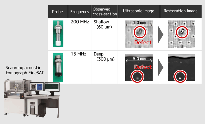
SAKAI"Image restoration" is a function that makes it easier to find defects by making ultrasonic inspection images appear clearer.
In the past, when trying to make ultrasonic images more visible, we used a method where we would increase the specifications of the probe, the point where ultrasonic waves are generated. By shortening the focal point of the beams or increasing the frequency of the ultrasonic waves, we narrowed the spread of the beams, decreasing the blurriness of images. However, as semiconductor ICs became smaller, we could not simply increase the specifications of the probe to detect defects. For example, if we increased the frequency, we were able to constrict the beam, but then the ultrasonic beams would not reach the back of the object being inspected. There were a few tradeoffs like this, and we had reached a limit in terms of hardware.
Here, we utilized software to make ultrasonic wave images clearer. Firstly, we used software to calculate the spread of ultrasonic beams based on the specifications of a given probe. As we can estimate the blurriness of images through the spread of ultrasonic beams, by adding image processing to the ultrasonic wave images, we figured we could eliminate the influence of blurs on images.
SAKAIPrecisely. In order to properly eliminate the influence of blurs on images, you must make adjustments to image processing based on the probes. But to do this, the specifications of the probes must be obtained.
Because the probes used for ultrasonic inspection equipment are usually manufactured at a different company from the one that manufactures the main apparatus, obtaining the specifications is not an easy task. However, in the case of FineSAT, the probes are developed in-house at Hitachi Power Solutions Co., Ltd. making it possible to obtain the specifications immediately. Although there are about 100 different types of probes for FineSAT, we obtain each of their specifications and adjust the equation by probe. In other words, image restoration is a technology that we were able to accomplish because we develop our probes in-house.
Figure 1: Sharpening ultrasonic images

SAKAIBased on a general equation, clarity improves by about 1.6 times. It is extremely difficult to achieve this through hardware. However, as this was accomplished through software, we are now able to capture clear images using this method even when using low frequency beams, that is to say, even with an ultrasonic beam that is widespread and reaches the back of the target.
SAKAIBecause we are inspecting for defects which cannot be seen with the naked eye, it was difficult because we did not know the right answer and could not confirm our results. Although we can estimate the blurriness from the specifications of the probes, in the end it is just a theoretical value, and in reality, each probe has its own "quirks." In order to ascertain these quirks, we intentionally embedded defects into semiconductor ICs and conducted inspections. We compared the actual images with how the embedded defects should appear based on calculations. We then slightly altered the image processing method and repeatedly adjusted them so the two would become closer and closer. By adjusting the model and changing the parameters, we learned each probe's quirks. However, this process did take a long time.
SAKAIAs I explained earlier, because of the changes in the manufacturing process of semiconductor ICs, we now need to find defects on entire wafers. In other words, we must somehow figure out how to find a contact lens that was lost on a baseball field. This is why "defect auto-detection" was developed.
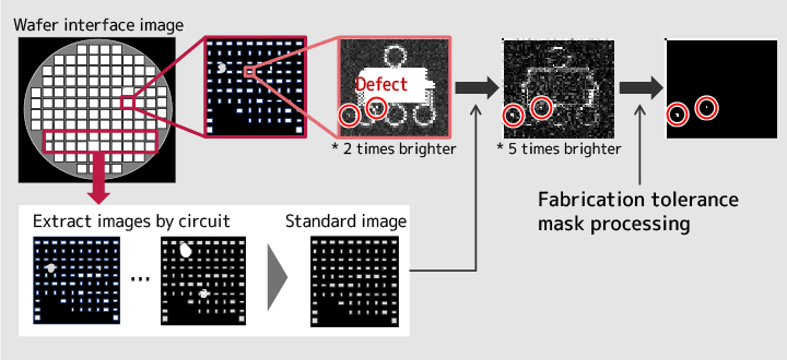
Semiconductor ICs are made by periodically burning circuit patterns on to wafers. During this process, if all the circuits are properly made, they should all have the same pattern. Thus, we extracted all the images of circuit patterns, computed statistical features, and then calculated the normal value (standard image). If any of these values deviate from statistical values, we determine that there is a defect.
However, an issue that occurs here is that circuit sizes vary, or are slightly different due to "fabrication tolerance." Here, the difference between fabrication tolerances and defects must be determined. Therefore, calculations were made beforehand determining how much noise will occur depending on how widespread the fabrication tolerance is, and based on these results they were masked. Through this, we were able to distinguish between noise generated by fabrication tolerance and defects, enabling us to properly identify defects.
Figure 2: Defect auto-detection

SAKAIThat's right. This function was a technology developed in response to a special request from a customer saying, "I would like to inspect all the circuit patterns while it is still a wafer." No other company's product has yet to implement a feature that can inspect all the circuits of a wafer at once.
SAKAIIt's the same as sharpening images, but again, it is the inability to know the right answer as we are inspecting for defects that cannot be seen with the naked eye. For example, even if a defect of 10 µm is detected, we cannot know for sure whether it is truly a defect unless we split the semiconductor IC open. As such, we sometimes split semiconductor ICs together with our customers in order to verify our inspection results. However, it is actually pretty hard to split them at only one cross-section… In fact, it's actually extremely difficult to cut something along a 10 µm defect! Sometimes the cross-section would be slightly off, displaying no defects. This is why we had our customers embed tiny defects and see whether we could detect them, or checked whether defects actually existed by examining the cross-sections with a scanning electron microscope (SEM).
SAKAIAs the share in Japan was originally about 70% to 80%, the share is currently expanding overseas, particularly in Asia. Although there are many manufacturers that handle the latter processes of semiconductor manufacturing in Asia, many of these locations still use visual observation for all inspections. These are the kinds of places where the share of FineSAT are expanding.
Moreover, many designers are using FineSAT to build safety features into their products. FineSAT gives feedback in the manufacturing process in that people can learn what kind of manufacturing processes generate certain defects. This is particularly important for automobile manufacturers. If one part of an automobile has a defect, it can lead to recalls and serious accidents. FineSAT enables inspection at the manufacturing stage for safety and security.

SAKAII believe so. However, as electronic parts such as semiconductor ICs continue to evolve in the future, ultrasonic inspections will only become more and more difficult.
Up until now, hardware improvements of probes and the like were the main types of improvements in the world of ultrasonic waves. In contrast to this, software utilization lags slightly behind. I still think there is much that can be done using software. From now on, I think that we should not only wait for requests from our customers, but readily anticipate our customers' needs. I think there is a need for our researchers to suggest ideas saying, "We need this kind of feature," and create new applications.
SAKAII hope to continue to probe into this technology that allows us to see what cannot be seen. This technology is not limited to ultrasonic waves, and I could even pursue X-rays or neutron beams. I also believe that this could be used not only for electronic parts such as semiconductor ICs, but for things that are even more relevant to our daily lives such as food products. I hope to continue to hone the technology of showing the accurate state of things by clearly displaying the inside of objects, enabling proper management.